Bharat Semi Raises $24 Million for Programmable AI Image Sensors: How On-Sensor Inference Cuts Edge Latency and Power Burn
Conventional computer vision pipelines waste power and time by streaming raw, high-resolution video frames from a camera sensor across a circuit board to an external processor before running a single neural network layer. On November 16 and 17, 2026, New Delhi and Bengaluru semiconductor startup Bharat Semi moved that architecture into the spotlight after closing a $24 million all-equity seed round led by Info Edge, South Park Commons, and IndusBridge Ventures to build programmable AI image sensors.
The verdict is clear: moving early visual inference directly onto the silicon die that captures light reduces data movement, board footprint, and system power consumption for battery-operated cameras, drones, and industrial robotics. For hardware engineers and product teams in India evaluating edge vision architectures, however, on-chip sensor compute introduces strict memory ceilings, custom toolchain dependencies, and commercial timeline constraints that require careful evaluation before committing to a bill of materials.
1. What Changed in Bharat Semi’s On-Sensor AI Architecture
Founded in late 2021 by Vrinda Kapoor and Vinayak Dalmia with former OmniVision executive Boyd Fowler serving as CTO, Bharat Semi operates across New Delhi, Bengaluru, and Santa Clara with roughly 75 employees. According to reports from TechCrunch and TechNode Global, the company integrates pixel capture, image signal processing, and programmable AI execution on a single fabless chip.
- Customer Design Wins: Bharat Semi has secured early design wins with US unmanned systems manufacturer General Atomics and India’s Kaynes Semicon. In semiconductor procurement, a design win confirms that an engineering team selected the sensor for an upcoming product architecture rather than immediate volume shipments.
- Development Timeline: First-generation silicon is currently in prototyping, second-generation prototypes are scheduled for mid-2027, and commercial volume production is targeted for late 2027.
- Fabless Business Model: The $24 million seed capital funds engineering expansion and sensor tape-outs while outsourcing wafer fabrication. Bharat Semi’s separate semiconductor fabrication facility proposal, developed with a US Space Force technology partnership, remains distinct and is not financed by this round.
2. Four Practical Steps for Engineers Evaluating Edge Vision Sensors
If you design smart surveillance cameras, warehouse robotics, or autonomous inspection rigs in India, you can prepare your firmware and model pipeline for in-sensor compute right now by following four concrete steps:
- Profile sensor-to-SoC bus energy in your current design: Measure how much power your MIPI CSI-2 interface and host NPU consume simply ingesting idle background frames. In always-on security cameras and battery drones, up to 60 percent of system energy goes toward waking the host processor to inspect frames that contain zero events of interest.
- Partition your vision model into a two-stage cascade: Separate lightweight event detection (such as motion classification, person detection, or defect triggers) from heavy multi-class recognition. Run a quantized INT8 or INT4 trigger network under 500KB on the front-end sensor or low-power microcontroller, and wake the main system-on-chip only when confidence crosses your threshold.
- Benchmark vendor SDKs against standard ONNX or TensorFlow Lite exports: Programmable sensors rely on proprietary compilers to map neural operators onto in-pixel or near-pixel compute arrays. Before locking a component into your schematic, verify whether the vendor toolchain supports standard quantized ONNX graphs without manual assembly rewrites.
- Audit supply chain lead times and second-source options: Because programmable AI image sensors are still entering prototype validation through 2027, pair any early evaluation kit with a pin-compatible or software-abstracted fallback sensor from established suppliers such as Sony or OmniVision so production schedules stay insulated from tape-out delays.
3. Commercial Trade-Offs, Incumbent Pressure, and Ecosystem Context
Bharat Semi enters an image sensor market projected to reach $49.8 billion by 2030, where incumbents Sony and OmniVision already ship mature, automotive-qualified parts with deep optical supply chains. Company claims around lower system cost and reduced data movement have not yet been independently benchmarked in commercial deployments, and engineering teams will scrutinize dynamic range, low-light noise, and thermal drift once second-generation samples ship in mid-2027.
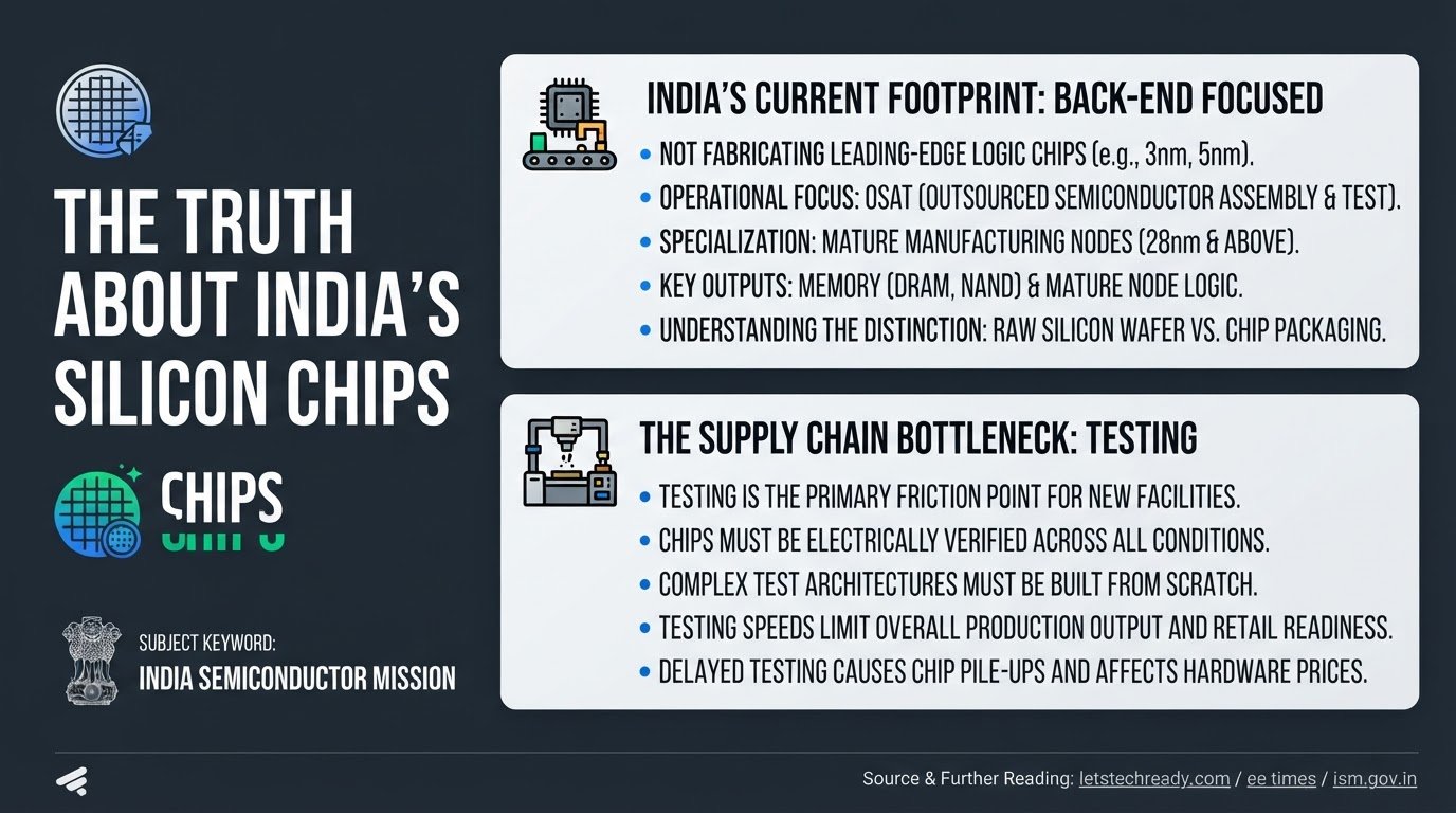
Near-term adoption targets consumer electronics and security surveillance before expanding into robotics, automotive, aerospace, and defense sockets, where environmental qualification cycles regularly span 18 to 24 months. Meanwhile, Indian electronics manufacturing partners such as Kaynes Semicon give local hardware startups an assembly and packaging path inside the country even while leading-edge sensor wafers are fabricated overseas.
At the same time, the funding coincides with broader momentum in India’s chip design ecosystem highlighted at the Bengaluru Tech Summit 2026, where Karnataka reported hosting more than 100 fabless semiconductor companies. By pairing domestic silicon design talent with outsourced foundry manufacturing, programmable edge sensors offer a capital-efficient path for Indian hardware startups to compete in global robotics, aerospace, and industrial automation sockets without waiting years for domestic wafer fabs to reach leading-edge nodes. Engineering teams tracking Indian semiconductor design programs and vendor qualification updates can follow upcoming sessions on the Bengaluru Tech Summit 2026 schedule.