

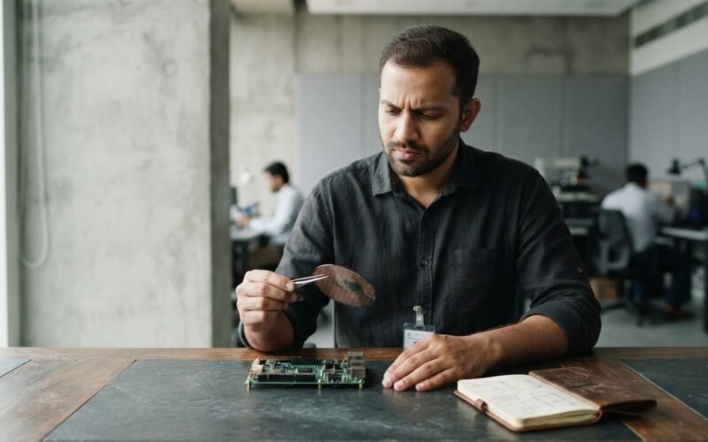
You are looking at the spec sheet of a new enterprise laptop or smartphone, trying to decode where its internal components actually come from. With headlines shouting about India's rapid rise in chip manufacturing, you might expect your next device to run on a processor entirely fabricated in Gujarat or Assam. The reality is more complex, leaving many tech buyers and businesses confused about when they will actually deploy hardware powered by Indian silicon.
The direct verdict is simple: India is not yet printing cutting-edge, sub-5nm smartphone brains or high-end AI processors. Instead, the India Semiconductor Mission is successfully establishing its foundation through back-end packaging, testing, and mature-node manufacturing. If you are planning hardware procurement or tracking tech timelines, you must separate early packaging milestones from actual front-end wafer fabrication to avoid supply chain misalignments.
Understanding the difference between the physical reality and the marketing hype requires looking at the actual milestones scheduled between October 11 and October 13, 2026. Here is the step-by-step breakdown of where India's silicon journey stands and how to align your hardware expectations.
1. Audit Active OSAT and ATMP Operational Status
The first step in evaluating India's chip capacity is understanding back-end manufacturing. Before a silicon chip can be slotted into a motherboard, it must undergo Outsourced Semiconductor Assembly and Test (OSAT) or Assembly, Testing, Marking, and Packaging (ATMP). This process takes raw silicon wafers, cuts them into individual dies, tests them for defects, and seals them in protective casings with electrical connections.
Currently, India's immediate operational output is concentrated in these back-end facilities rather than front-end wafer fabrication.
- Micron's Sanand Facility: Located in Gujarat, this plant is actively packaging DRAM and NAND flash memory. If your organization is procuring memory modules, some of the physical packaging and testing are happening here.
- Tata Electronics' Jagiroad Facility: Located in Assam, this facility focuses on packaging mature-node logic chips and display drivers.
To track how these packaging plants are scaling, you can read more about how India Semiconductor Mission: Five OSAT Plants Go Live to support global supply chains.
2. Track Front-End Wafer Fabrication Timelines
Front-end wafer fabrication is the highly complex process of printing microscopic circuits onto silicon discs. This is where the distinction between cutting-edge nodes (like the 3nm chips in premium smartphones) and mature nodes (used in cars, home appliances, and industrial equipment) becomes critical.
India's first major commercial wafer fabrication plant is the joint venture between Tata Electronics and Taiwan's Powerchip Semiconductor Manufacturing Corporation (PSMC) in Dholera, Gujarat.
- The Node Reality: The Dholera fab is designed for mature nodes, specifically 28nm, 40nm, 55nm, and 90nm chips.
- The Commercial Timeline: Do not expect mass-market Indian-fabricated processors in laptops or phones this month. The Dholera facility is targeting its first physical silicon runs by late 2026. Commercial volume ramp-up will follow in subsequent phases.
For a detailed breakdown of the construction progress and how these facilities compare, explore the analysis in From Dholera to Sanand: Inside India's Rapid Semiconductor OSAT and Fab Buildout.
3. Cross-Reference Equipment and Materials Supply Chains
A semiconductor fab cannot function without a highly specialized global supply chain of lithography machines, ultra-pure chemicals, and silicon wafers. When tracking the viability of India's silicon timeline, you must look at the arrival of these critical tools.
Two major supply chain developments are anchoring the physical construction of these plants:
- The Tata-ASML Agreement: Tata has secured partnerships with ASML, the Dutch giant that dominates the lithography machine market, ensuring the Dholera plant receives the advanced optical equipment needed to print circuits on wafers.
- Fujifilm's Materials Facility: Chemical supply chains are also moving closer to the factories. Fujifilm is scheduled to begin construction on a specialized semiconductor materials facility in October 2026, providing the local chemical infrastructure required for daily factory operations.
4. Map Sovereign Silicon Incentives Against the Fiscal Framework
For enterprise buyers and hardware developers, procurement strategies must align with the financial backing of these programs. The Indian government has updated its financial support structure to transition from basic incentives to long-term ecosystem development.
Under the Semicon 2.0 program, the government has approved a massive fiscal outlay of 1.275 trillion INR, which is approximately 13.23 billion USD. According to the official India Semiconductor Mission Portal, this funding is directed not just at building factories, but also at supporting local chip design startups, purchasing manufacturing machinery, and securing raw materials.
This financial backing ensures that the projects currently under construction have the long-term runway needed to survive the cyclical ups and downs of the global tech market, as detailed in India Briefing reports on Semicon 2.0.
To understand how these local policy shifts fit into the broader global context, you can read about India's Silicon Rise and the Global Chip Squeeze.
Summary for Tech Buyers and Consumers
If you are managing an IT department, purchasing enterprise hardware, or simply curious about when your personal devices will run on Indian silicon, keep these timelines in mind:
- Memory and Packaging (Now): Your devices may already contain memory or display drivers packaged at Micron's Sanand or Tata's Jagiroad plants.
- Mature-Node Logic (Late 2026 and Beyond): Domestic fabrication of 28nm to 90nm chips for automotive, power management, and IoT devices will begin pilot testing in late 2026.
- Leading-Edge Processors (Post-2028): High-end CPUs and GPUs for smartphones and laptops will continue to rely on global foundries in Taiwan and the US for the foreseeable future.
Verify the exact manufacturing origin of your hardware components by checking the detailed component sheets provided by your enterprise suppliers.
