You are reading the specifications of your next smartphone, smart TV, or office laptop, and you see announcements about domestic hardware production. You might wonder if India is already manufacturing the ultra-thin, sub-7nm brain chips that run high-end devices, directly competing with legacy giants in Taiwan or the United States.
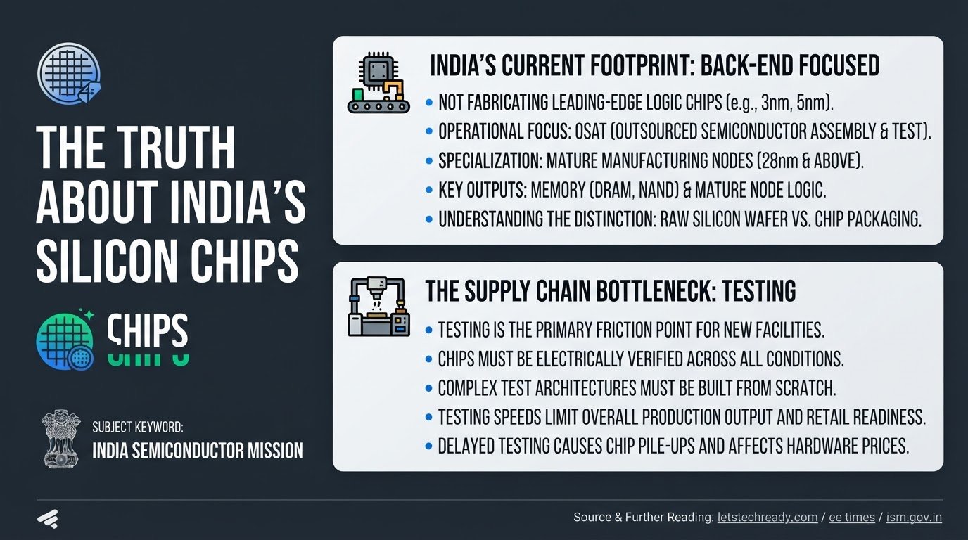
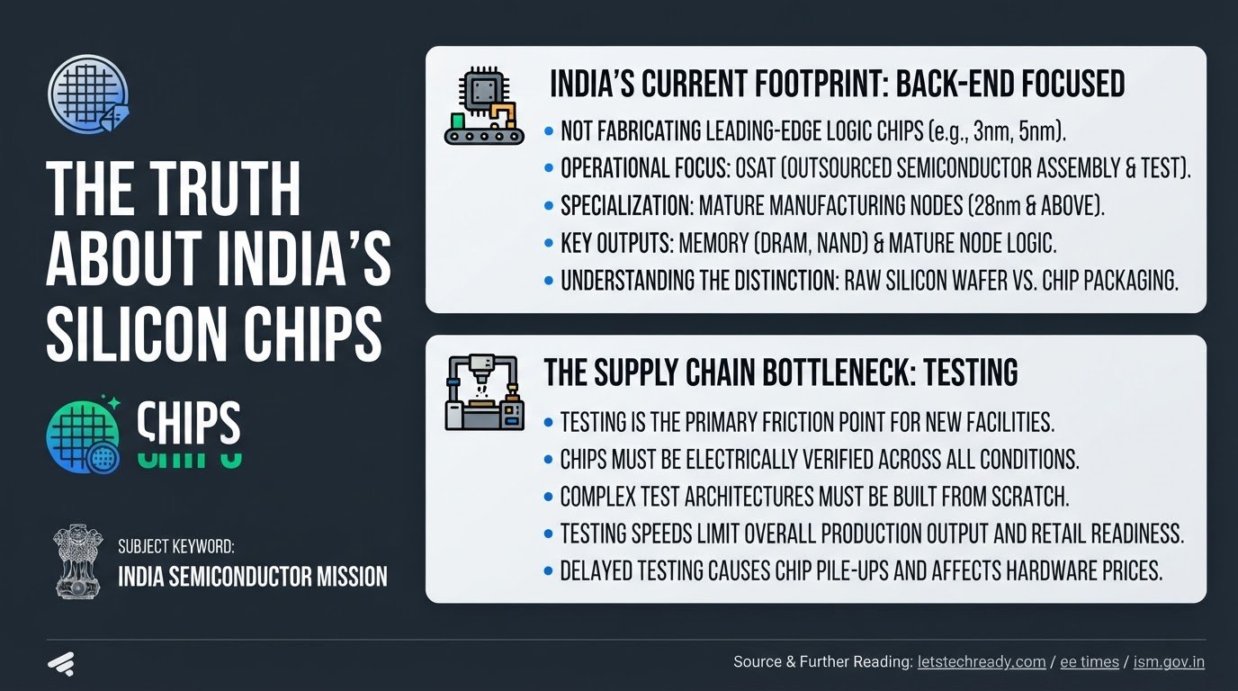
The short answer is no. India is not currently fabricating leading-edge logic chips. The country's immediate operational footprint under the India semiconductor mission is focused on Outsourced Semiconductor Assembly and Test (OSAT) facilities and mature manufacturing nodes of 28nm and above.
Instead of carving microscopic transistors onto raw silicon wafers, Indian facilities are mastering the critical back-end process: taking wafers made abroad, cutting them, packaging them, and testing them to ensure they work reliably in everyday hardware. Understanding this distinction helps you make informed purchasing decisions and understand the actual timeline of global hardware manufacturing.
The Reality of India's Silicon Footprint
There is a common consumer myth that "packaged in India" means the silicon wafer itself was fabricated domestically. In reality, raw silicon wafer fabrication and chip packaging are two entirely different steps in the supply chain.
Raw fabrication requires multi-billion-dollar factories called fabs, which print microscopic circuits onto silicon. Packaging, or OSAT, is the subsequent step where those fragile silicon wafers are cut into individual dies, wired into protective casings, and prepared for installation on device circuit boards.
Currently, India's active facilities are focused on these back-end processes and mature nodes. For example, Micron's Sanand plant packages DRAM and NAND memory, which are essential for storage and temporary memory in computers and phones. Meanwhile, Tata's Jagiroad facility handles mature node logic and display drivers, which power screens and basic electronic controls rather than high-end computer processors.
To see how these facilities fit into the broader national strategy, you can read about the transition as five OSAT packaging plants go live across the country.
Why Testing is the Real Supply Chain Bottleneck
The primary friction point for new packaging facilities is not just putting the chips into plastic or ceramic housings: it is testing them fast enough. Every single chip must be electrically verified across different temperatures and workloads before it can be shipped to device manufacturers.
According to reports on EE Times, Indian OSATs must build complex test architectures from scratch to meet production targets. If testing speeds do not match packaging speeds, chips pile up in warehouses, delaying the release of local hardware and impacting retail prices. You can explore how these supply chain dynamics influence retail tech costs in our analysis of rising PC and device prices.
How to Verify the Origin of Your Device's Silicon
If you want to track where your device's internal components actually come from and understand the progress of sovereign silicon, you can follow these four practical verification steps.
1. Verify the Facility Status
Check the official India Semiconductor Mission Portal to distinguish between active OSAT packaging plants and fabs that are still under construction. While packaging plants are actively processing memory and mature logic, major fabrication projects, such as Tata's Dholera wafer fab, are still in their construction and tooling phases.
2. Audit the Chip Type and Node Size
When a device is marketed as containing domestic silicon, look up the specific processor or memory module online. According to supply chain data from Zetwerk, components packaged domestically are memory modules or mature node logic (28nm or larger). They are not the 3nm or 5nm main processors found in flagship smartphones. To set realistic expectations for when these components will reach your hands, consult our guide on realistic timelines for Indian silicon.
3. Track Global Equipment Lead Times
The timeline for building advanced fabs depends heavily on lithography machine deliveries from global suppliers like ASML. You can monitor global foundry equipment bookings and tool delivery schedules through industry trackers like The Elec. If global equipment lead times stretch past 18 months, domestic fab completion dates will likely shift accordingly.
4. Check the Testing Integration
Look for partnerships between local packaging providers and established test system manufacturers like National Instruments. A packaging plant that has fully integrated automated test equipment is far more likely to deliver stable, defect-free components to the consumer market without causing local shipping delays.